
Paper presented in the 12th IET International Conference on AC and DC Power Transmission, 28-29 May 2016, Beijing, China, organized by The Institution of Engineering and Technology (IET), U.K., co-organized with Tsinghua University

Abstract:
Recent year, Multilevel Modulation Converter (MMC) topology has motivated the development of VSC-HVDC system greatly. This paper shows the relationship between transmission line current and IGBT rated current in different packages and voltage classes for VSC-HVDC application. Different semiconductor solutions for future high power systems are compared on their relevant parameters and characteristics, especially for strengths and weaknesses between PressPack IGBT and Wire-Bond IGBT in chip-level current sharing and reliability consideration. The latest development in IGBT chip and package technologies of Reverse Conducting IGBT with Diode Control (RCDC) and XHPTM are introduced. Experimental results show good current sharing amongst paralleled XHPTM modules, opening the path as solution for future high power VSC-HVDC system.
1. Power device rating requirements in VSC-HVDC systems
MMC topology imposes special application requirement to IGBT due to the arm current of sub-modules differs from conventional 2-level converter by having DC component [1], thus causing unbalance in load current and power losses. The bottom devices T2 and D2 are operating with high duty-cycle in inverter and rectifier side respectively and thus generating significantly higher power losses.

Normally, the modulation index m is set to approximately 0.9 to give 10% margin to avoid over-modulation, and cosψ is defined as 0.9 for reactive power capability in most installations. Therefore, the peak arm current Ia peak can be derived as 1.2 times of DC transmission current, which is not fixed but depending on reactive power demand level.
The relationship between transmission line current IDC and IGBT rated current ICNOM is analyzed with limiting factors of operating Tvj and switching SOA, it is also dependent on the VCE voltage class (3.3~6.5kV) and housing(IHV-A,IHV-B) with different Tvjmax. Recently, next generation of VSC-HVDC system rated at ±500kV/3000MW is being announced and planned with IDC at 3000A, which requires IGBT modules with a current rating far beyond the available limit today.
There are several possible approaches to address the demand for high voltage (Vce class ≥3.3kV) IGBT module to realize such system with power devices at ICnom = 3000A.
A. Paralleling of IGBT module in wire-bond technology
B. IGBT in PressPack technology
C. IGCT in PressPack technology

2. Comparison of power device solutions
At present, the two key technologies for full-controlled high power semiconductor are (a) voltage-controlled IGBT with multiple chips in parallel, and (b) current-controlled IGCT in single wafer, and are further classified into PressPack type and wire-bond type according to packaging technology chosen.
It is well known that PressPack IGBT have good thermal performance due to double-sided cooling and short circuit failure mode (SCFM) to avoid arcing upon failure, however some issues do exist at system level.
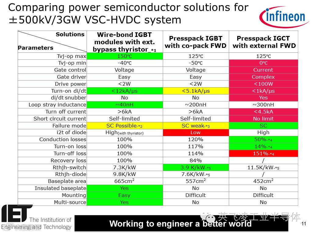
IGCT:Although the IGCT has a significant advantage in power losses and with SCFM feature which are the top requirements for power transmission and distribution systems, several restrictions still limit its application. It is not recommended to be used into VSC-HVDC system due to:
A. The minimum operating temperature of IGCT should be above 0℃ due to the electrolytic capacitors in its driver stage, which also poses risk of failure.
B. The maximum turn on di/dt is set to 1kA/μs being limited by the spreading rate of its conductive region. An additional inductor is thus required in series to reduce current rise slew rate, which also bring a high voltage spike during turn off and RCD snubber is required to clamp such overvoltage. Such clamping and snubber circuit will increase the volume and cost of the sub-modules.
C. Furthermore, the IGCT is unable to limit the short circuit current during arm short-though, and may even not be able to turn off over current during system fault, which pose safety concerns for system protection.
IGBT:Both wire-bond IGBT and PressPack IGBT are constructed by multiple chips connected in parallel inside their packages. High power semiconductor is a complex paralleling “system” rather than a simple “component”.
2.1 Circuit model and current sharing amongst chips
PressPack IGBT:There is only one emitter terminal use for both power flow and gate signal reference. This will lead to gate-emitter voltage differences especially during switching, and thus cause uneven current sharing amongst chips at different physical positions. Such imbalance in current and losses may lead to thermal hot spots and reduced lifetime of the power devices. An improvement approach using a complex bus-bar has been proposed, which is a challenge in mechanical design and maintenance, and will reduce thermal performance to single-sided cooling only. [6]
The problem of mechanical stress can be solved by adopting springs to connect the chips and baseplate. In case of a single chip failure, there is risk of insufficient pressure to provide sufficient metal-to-metal contact area. Therefore, this approach poses risk of robust SCFM feature under large and prolonged fault current.
Wire-bond IGBT:A dedicated gate signal path via auxiliary emitter can be arranged to give symmetric layout for chips to achieve equal gate-emitter voltage amongst chips during switching. The parasitic inductance in the collector and emitter paths can also contribute to the commutation loop symmetry for chips inside:
Symmetric drive path design
Symmetric load current path design
Minimize communication loop area (Small stray inductance)
Good performance in current sharing amongst chips
Though the bond wire maybe burnt out by overcurrent and the wire-bond IGBT cannot guarantee a robust SCFM feature, the Presspack bypass thyristor installed in the MMC submodule output will be triggered on during failure, thus offering alterative form of safe design in system level.

2.2 Reliability consideration
IGBT module are constructed by chips connected in parallel, higher current ratings are achieved by increasing the number of chips paralleled, and FIT rate will be increased proportionally (1 FIT=1 failure per 10^9 operating device-hours). In addition to chip technologies, the package should:
Ensure internal current sharing amongst chips in static and dynamic operations;
Relieve mechanical stress frommounting;
Offer highly reliable electrical connection.

The factors (B) and (C) above have less effect on wire-bond IGBT.
To verify power semiconductor device reliability performance, large resources over long time are both needed. The most accurate approach to evaluate power semiconductor device reliability is by statistical analysis on field failure data of same type of chip technology (e.g. 3.3kV Generation 3 chips) applied to the same application (e.g. VSC-HVDC).
For most power system equipment, it is required to establish reliability model for failure prediction and calculation from the onset. However, semiconductor suppliers are often unable to provide such data or reliability model for new application (e.g. VSC-HVDC) when field data is missing or statistically insufficient. As compromise, field failure statistical data from other applications had to be used, causing errors in the build-up of reliability model and the prediction results thus derived.
Furthermore, it is sometimes found that DC stability specification of power semiconductor device is being mistakenly used for reliability prediction. It should be noted that the objective of DC stability test is to verify the failure probability of power semiconductor device under the effect of cosmic radiation, in which multiple chips in parallel are being irradiated by high-energy protons or neutron to simulate the influence of cosmic radiation on failure. The test result is highly sensitive to applied DC voltage and weakly correlated to junction temperature. Limited by energy level of irradiation equipment, the test criteria is often set to 100 FIT. Amongst other factors, failure rate related to DC stability test is proportional to the total active chip area while independent of the package technology used. Cosmic radiation failure rate represented by DC stability test is only a part of the total failure rate, therefore it should be used only for DC operating voltage selection but not for overall system reliability evaluation. Accurate reliability prediction model for power semiconductor device for VSC-HVDC system application is needed but missing right now.

3. IGBT chip technologies development
One approach to increase the current density of IGBT power modules is to integrate the IGBT and freewheeling diode functionally and monolithically. Such technology is known as Reverse-Conducting (RC) IGBT. The latest technology in RC-IGBT is to incorporate gate control to diode characteristics. Such technology is called Reverse Conducting IGBT with Diode Control (RCDC)[7-9].
In addition to the substantial increase of IGBT current rating in the same package, further advantages with RCDC technology are:
A. Significantly improved Rth and Zth of IGBT and diode
B. Significantly increased diode chip area and thus i²t
C. Reduced recovery losses by diode control
D. Reduction of Tvj ripple due to thermal cross-coupling of IGBT and diode, and increase lifetime
In the conventional 6.5kV 750A IGBT module in 190×140mm² industry-standard package, the current rating will be up to 1000A when using RCDC chips instead.

RCDC provides an option to use gate-control to optimize the diode characteristics for low VF during diode conduction (with VGE= -15V) and low Erec during switching (with VGE=+15V).
RCDC gate control: A desaturation pulse (red) will be applied to the bottom “diode” with pulse width t_desat at a locking time t_lock prior to diode recovery by the turn-on of the top “IGBT” gate signal (in blue).

4. IGBT package technologies development
New high-voltage package called XHPTM[10-11] is being proposed recently. Such module package is designed for scalability by sample paralleling. The new XHPTM package offers several special features:
Scalable package designed for paralleling
One package platform covering all voltage classes from 3.3kV to 6.5kV
Half-bridge configuration, instead of the single-switch configuration common in high-voltage IGBT modules,
Low internal package stray inductance prepared for future high-speed switching devices
Widely-separated DC & AC terminals to facilitate busbar layout to minimize stray inductance
All these features together lead to a significant reduction of internal (module package) and external (bus bar) stray inductance, estimated to be about 1/6 of that from existing IHV-B package.
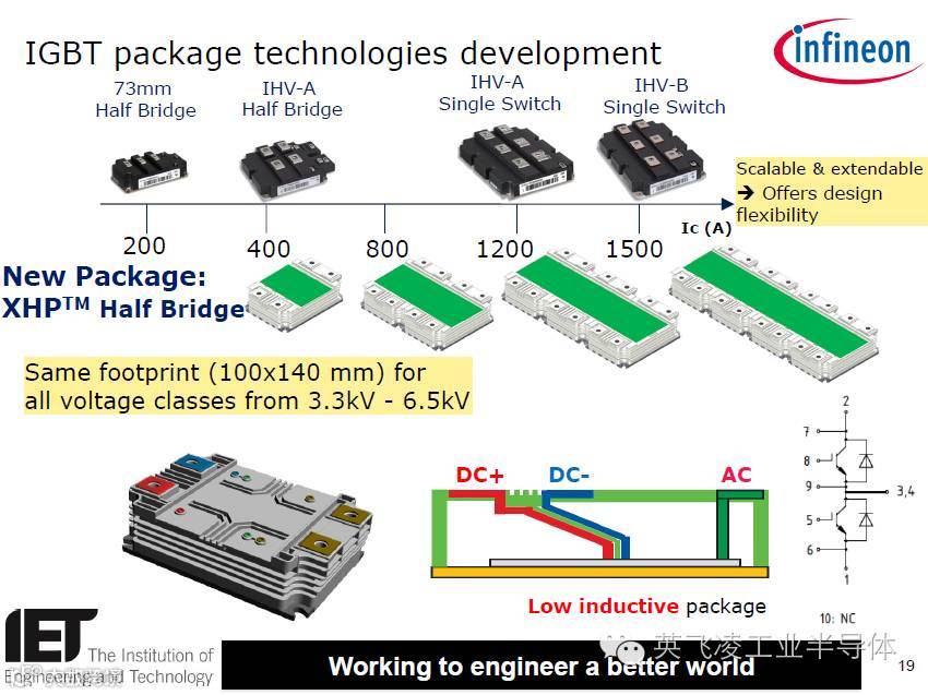
Compared to the standard IHV-B package, such lower stray inductance will reduce turn-off Vce overshoot by approx. 30% and reduce turn off loss by over 5%. Meanwhile, IGBT could be turn on faster with turn on loss reduced by approx. 21% while keeping the same electrical stress level in diode during reverse recovery.

To verify the current sharing performance of paralleling the new XHPTM modules, 4 units of 3.3kV/ 450A half-bridge modules are connected in parallel. The maximum dynamic current imbalance is only 2.7% (defined as the max. current difference amongst modules divided by sum of all currents in the modules).

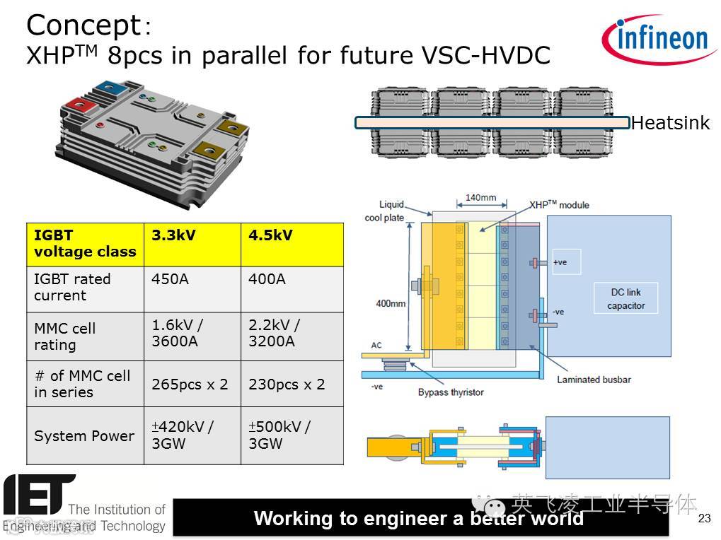
5. Solution for future 3GW VSC-HVDC system
As explained in Section 2 before, the reliability of multiple wire-bond IGBT modules in parallel is not inferior to a single PressPack IGBT device when other factors are the same, while internal current sharing amongst chips is ensured by independent and symmetric gate drive paths and symmetric load current paths. Therefore, using 8 units of XHPTM in parallel would be the a competitive solution for future 3GW VSC-HVDC application.
Product ratings of 3.3kV/450A and 4.5kV/400A will be offered in XHPTM package, which enable MMC submodules with capacities up to 1.6kV/3600A and 2.2kV/3200A respectively be built, and subsequently be used to construct ±420kV/3GW or ±500kV/3GW VSC-HVDC systems.
Acknowledgements
The authors gratefully acknowledge Mr. Yimeng Shi of Firstack for designing the gate driver and module adaptor boards and perform the module paralleling current sharing test.
References
[1] M. Davies, M. Dommaschk, J. Dorn, J. Lang, D. Retzmann, D. Soerangr, “HVDC PLUS – Basics and Principle of Operation”, Siemens, (2008)
[2] Tomas Modeer, Hans-Peter Nee, Staffan Norrga, “Loss Comparison of Different Sub-Module Implementations for Modular Multilevel Converters in HVDC Applications” EPE Birmingham, (2011)
[3] Ke Ma, Frede Blaabjerg,“The Impact of Power Switching Devices on the Thermal Performance of a 10 MW Wind Power NPC Converter”, Energies, 5, 2559-2577, (2012)
[4] Eric Carroll, Norbert Galster, “IGBT or IGCT: Considerations for Very High Power Applications”, European Power Semiconductors Forum, (1997).
[5] Simon Eicher, Munaf Rahimo, et al, “4.5kV Press Pack IGBT Designed for Ruggedness and Reliability”, IAS Seattle, USA, (2004)
[6] A. Müsing, et al, “Optimization of the Current Distribution in Press-Pack High Power IGBT Modules”, International Power Electronics Conference, (2010).
[7] Dorothea Werber, et al, “6.5kV RCDC for Increased Power Density in IGBT-Modules”, ISPSD, Waikoloa, Hawaii (2014).
[8] Dorothea Werber, et al, “A 1000A 6.5kV Power Module Enabled by Reverse-Conducting Trench-IGBT Technology” PCIM Europe, Nuremberg (2015).
[9] Daniel Domes, "Control Method for a Reverse Conducting IGBT", PCIM Europe, Nuremberg (2015).
[10] Thomas Schütze, et al, “Boost Your System! Defining the Future of IGBT High-Power Modules”, Bodo´s Power Systems, March (2015).
[11] Sven S. Buchholz, et al, "Electrical performance of a low inductive 3.3kVhalf-bridge IGBT Module", PCIM Asia, (2015).
[12] http://www.firstack.com
