


GLOBAL PCB DAILY
全球PCB行业每日动态
2026年10月21日(周三)|近24小时 中英双语
今日焦点 国内·投资/材料 10月20—21日
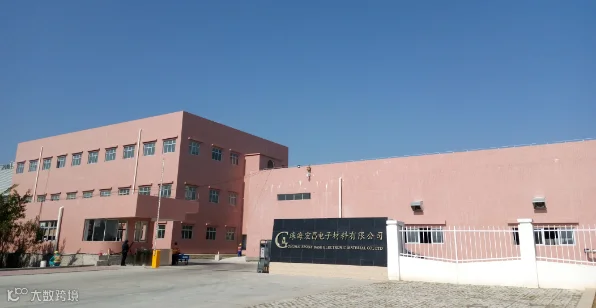
宏昌电子在珠海一口气上三个项目,12.6亿元从高端覆铜板铺到先进封装膜材
宏昌电子10月20日盘后连发三份公告,全部落在珠海经济技术开发区,协议投资金额合计不低于约12.6亿元,董事会已审议通过,不用上股东会。
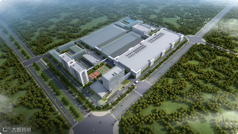
最大的一笔是「珠海宏仁高端覆铜板及半固化片建设项目」,投不低于8亿元,其中固定资产投资不低于7亿元、设备投资不低于6亿元,占地约3.5万平方米,主厂房加公用、环保工程建筑面积不低于3.6万平方米。达产后新增年产高端覆铜板1080万张、半固化片2400万米,全部投产预计年产值超8.8亿元、年税收约3900万元。
第二笔是「珠海宏仁二期扩建自动化及智能制造项目」,投不低于1.9亿元,用现有位于金湾区南水镇洁能路169号的4.7万平方米厂房扩产,达产后年新增高阶覆铜板240万张、半固化片720万米,计划2028年6月30日前投产。两块加起来,高端覆铜板年产能新增1320万张、半固化片3120万米。
真正值得盯的是第三笔:2.7亿元的先进封装膜材(GBF)项目,新建年产384万平方米产能,建设周期24个月。GBF是ABF积层膜的国产替代路线之一,目前大陆走这条线的还有华正新材料的CBF、深圳新宙邦的NBF,三家里CBF走得最快,GBF此前处于小批量试产阶段。宏昌从环氧树脂做到覆铜板,再往封装膜材伸手,这一步跨得比同行大。
公告里也把话说在前面:三个项目都还要过环评、安评、能评,用地手续没办完,投资额、建设周期和产值都是预估数。
出处:公司公告(巨潮资讯网)、证券时报e公司、每日经济新闻,2026年10月20日盘后公告/10月21日披露
EN | Hongchang Electronics disclosed three investment agreements late on Oct 20, all sited in Zhuhai Economic and Technological Development Zone, with combined committed investment of no less than about RMB 1.26 billion; the board approved all three, with no shareholder vote required. The largest is a high-end copper-clad laminate and prepreg project of at least RMB 800 million (fixed assets at least RMB 700 million, equipment at least RMB 600 million) on a 35,000 sqm plot, adding annual capacity of 10.8 million high-end CCL sheets and 24 million metres of prepreg at full run, with projected output value above RMB 880 million and tax of about RMB 39 million. A second-phase automation and smart-manufacturing expansion of at least RMB 190 million reuses an existing 47,000 sqm plant in Jinwan district, adding 2.4 million CCL sheets and 7.2 million metres of prepreg, with production due before June 30, 2028. Together the two add 13.2 million sheets of high-end CCL and 31.2 million metres of prepreg a year. The third project is the one to watch: RMB 270 million for advanced packaging film (GBF), with 3.84 million sqm of new annual capacity over a 24-month build. GBF is one of China's candidate replacements for Ajinomoto build-up film, alongside Huazheng New Materials' CBF and Shenzhen Capchem's NBF; CBF is furthest along and GBF had been at small-batch pilot stage. Moving from epoxy resin to CCL and now into packaging film is a bigger step than most domestic peers have taken. The filings caution that all three still need environmental, safety and energy assessments, that land procedures are incomplete, and that investment, timelines and output figures are estimates.
今日焦点 国外·供需/设备 10月20—21日
缺料从载板蔓延到设备与耗材:关键设备交期拉到30个月,CoWoS扩6.8倍载板只翻倍
欣兴电子董事长简山杰在TPCA Show上的一组数字,被TrendForce在10月20日整理成报告,读起来比现场演讲更扎眼。
缺料的范围已经不是载板本身。低CTE玻纤布、CCL、ABF三类材料同时吃紧;设备端更麻烦,超过80%的关键设备交期被拉长,其中超过20%的品类交期翻了一倍以上,部分拉到30个月——两年半。原因是供应商的供应商扩产跟不上,一级供应商想加产能也加不动。
更值得琢磨的是扩产倍数的错位:到2028年,CoWoS产能相对2024年要长6.8倍,超大规模云厂商资本支出长6.3倍,DRAM产能长1.8倍,而IC载板产能只翻一倍。基数不同不能直接划等号,但节奏上的落差摆在那里。
尺寸也在往大里走。载板从早期的1倍光罩面积,到2025年3倍,2026年目标5倍,2027—2028年5到9倍,最终可能到12—14倍。AI芯片电流已经动辄超过1000安培,供电完整性、高速信号、热管理和热机械可靠性一起上难度,面积一大,单片良率和单条产线产出都会被拉低。
英特尔EMIB这条链的良率最能说明问题:业界消息称目前约45%,目标是2026年第四季度到50%、2027年第一季度到60%。下游已经在用长约锁产能,今年春天就有客户跟欣兴谈长达七年的协议,一部分还是预付款。味之素的ABF积层膜和日东纺的T-Glass这两样,暂时找不到替代方案。
出处:TrendForce,2026年10月20日;EMSNow同日转载;快科技,2026年10月21日
EN | TrendForce on Oct 20 pulled together figures from Unimicron chairman S.C. Chien's TPCA Show remarks, and in aggregate they land harder than the speech itself. The shortage is no longer about substrates alone: low-CTE glass cloth, CCL and ABF are all tight at once, while more than 80% of critical equipment has seen lead times stretch, over 20% of categories have more than doubled, and some now run to 30 months — two and a half years. The cause sits a tier up: the suppliers' suppliers cannot expand fast enough, so even first-tier vendors cannot add capacity. The bigger issue is the mismatch in expansion multiples. By 2028, CoWoS capacity is set to grow 6.8x from 2024, hyperscaler capex 6.3x and DRAM 1.8x, while IC substrate capacity merely doubles. Different bases mean the multiples are not directly comparable, but the gap in pace is real. Substrates are also getting bigger: from roughly 1x reticle size in early designs to 3x in 2025, 5x targeted for 2026, 5-9x in 2027-2028 and potentially 12-14x eventually. AI chips already draw well over 1,000 amperes, pushing power integrity, high-speed signalling, thermal management and thermomechanical reliability at once, and as area grows, per-panel yield and line output both fall. Intel's EMIB chain shows the yield strain: industry sources put current yields near 45%, with targets of 50% by 4Q26 and 60% by 1Q27. Customers are already locking capacity through long-term agreements — some approached Unimicron as early as this spring about seven-year deals, part of it prepaid. Ajinomoto's ABF film and Nitto Boseki's T-Glass remain without viable substitutes.
3 国内·产能/供应链 10月21日
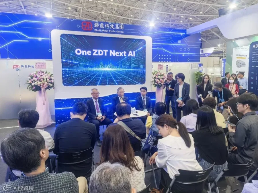
臻鼎沈庆芳在TPCA现场:客户从「去中国化」转向供货能力优先,泰国配套跟不上
全球PCB龙头臻鼎科技集团董事长沈庆芳在TPCA Show期间受访,一句话概括当下的心态:「以后速度慢的人可能会比较吃亏,因为时间不能等。」
他说臻鼎光模块相关业务今年较去年翻倍成长,明年也会维持倍数级成长。鹏鼎深圳第三园区投资逾100亿元人民币,今年7月已经动土,是臻鼎往AI高阶市场走的关键布局。
关于供应链迁移,他给了一个不太一样的观察:过去客户对产业链的「去中国化」要求,近一年已经转向供货能力优先。这几年不少PCB企业跑去泰国设厂,但当地产业链不完整,材料、设备和配套都不足,很难快速建立稳定的量产能力,客户没法无限期等下去。
大陆这边他能报出的数字是:臻鼎有超过两万名大陆工程师,今年又在大陆招了2363名大学本科毕业生,其中近三分之一来自双一流高校——「所以扩厂会那么快」。同场展出的大族数控也提到,进入AI时代后与台企的合作反而更紧密,这家深圳企业目前是全球最大的PCB专用生产设备制造商,持有2000多项专利。
出处:中新社,2026年10月21日(台北TPCA Show展会现场采访)
EN | Zhen Ding Technology chairman Shen Ching-fang, speaking during the TPCA Show in Taipei, summed up the mood in one line: from here on, the slow ones lose, because time does not wait. He said Zhen Ding's optical-module-related business has doubled this year over last, and will keep growing at multiples next year; the group's Pengding Shenzhen third park, with investment above RMB 10 billion, broke ground in July and is the core of its push into high-end AI boards. On supply-chain relocation his read differs from the usual narrative: over the past year, customers have shifted from demanding de-Sinicisation to prioritising delivery capability. Plenty of PCB makers have moved into Thailand, he noted, but the local chain is incomplete — materials, equipment and supporting services are all thin, making stable volume production hard to stand up quickly, and customers cannot wait indefinitely. On the mainland side he cites more than 20,000 engineers at Zhen Ding and 2,363 new university graduates recruited this year, nearly a third from Double First-Class schools, which he says is why the plants go up so fast. Also on the show floor, Shenzhen's Han's CNC — now the world's largest maker of PCB-specific production equipment, with over 2,000 patents — said cooperation with Taiwanese peers has actually tightened in the AI era.
4 国内·资本/扩产 10月20—21日
奥士康要发H股去香港,湖南、广东、泰国三个基地之后的下一步
奥士康10月20日盘后公告,董事会审议通过发行H股并在香港联交所主板上市的议案。发行股数不超过发行后总股本的20%(超额配售权行使前),并可授权整体协调人行使不超过前述股数15%的超额配售权,方式为香港公开发售加国际配售。
募资用途写得很清楚:产能建设升级、加大研发投入、未来潜在并购及战略投资、补充营运资金。安永已被聘为审计机构。这事还要过股东会,并拿到中国证监会、香港联交所和香港证监会的批准或备案。
奥士康的主业是PCB,产品用在数据中心及服务器、汽车电子、通信和消费电子,目前有湖南、广东、泰国三大生产基地,走「一地集成化设计、多地制造」的模式。泰国基地是行业里较早实现海外投产的之一。同日,公司10亿元的奥士转债也在深交所上市。
对国内PCB厂来说,A+H这条路的现实意义在于海外产能和海外客户:泰国基地要继续投、海外客户要就近交付,港币融资通道比单纯靠境内再融资灵活。
出处:每日经济新闻,2026年10月20日盘后公告/10月21日报道
EN | Aoshikang announced after market close on Oct 20 that its board has approved a plan to issue H shares and list on the Main Board of the Hong Kong Stock Exchange. The issue will not exceed 20% of post-issue total share capital before any over-allotment, with an overall coordinator authorised to exercise a greenshoe of up to 15% of that amount, via a Hong Kong public offer and international placement. Use of proceeds is spelled out: capacity construction and upgrading, higher R&D spending, potential future M&A and strategic investments, and working capital. Ernst & Young has been appointed auditor. The plan still needs shareholder approval plus clearance or filing with the CSRC, HKEX and the SFC. Aoshikang makes PCBs for data centres and servers, automotive electronics, communications and consumer devices, running three bases in Hunan, Guangdong and Thailand under a 'design in one place, build in many' model; its Thai site was among the earliest overseas PCB plants in the industry to reach production. Separately, its RMB 1 billion convertible bond listed on the Shenzhen exchange the same day. For Chinese PCB makers, the point of an A+H structure is overseas capacity and overseas customers: funding a Thai build-out and serving customers locally is easier with a Hong Kong dollar channel than with domestic refinancing alone.
5 国内·融资/出海 10月21日
满坤科技7.6亿元可转债上市,5.02亿元砸向泰国年产110万平方米高端PCB
满坤科技7.6亿元可转债(满坤转债,代码123287)10月21日在深交所上市,发行760万张,其中向原股东优先配售6.18亿元、占发行总量81.32%,网上投资者认购1.4亿元。中证鹏元给的主体及债项评级为AA-,展望稳定。
钱分两处。大头是泰国高端PCB生产基地,总投资约5.02亿元、拟用募集资金4.7亿元,选址泰国巴真武里府304工业园区,规划年产110万平方米高端印制电路板。另一笔是智能化与数字化升级改造,总投资约3.05亿元、拟用2.9亿元,主要买高自动化高精度智能设备、搭数字化管理系统、补信息安全能力。
公司给的说法是,泰国基地一方面靠「海外产能卡位」接住AI服务器电源这块的客户积累,另一方面跟国内产能形成互补;智能化改造则是把现有基地的高端产品交付能力提上去。这也是今年PCB厂再融资里很典型的组合:一手出海,一手提效。
出处:证券时报,2026年10月21日
EN | ManKun Technology's RMB 760 million convertible bond (ManKun CB, code 123287) listed on the Shenzhen Stock Exchange on Oct 21, issued as 7.6 million bonds, with RMB 618 million — 81.32% of the total — allocated preferentially to existing shareholders and RMB 140 million taken up by online investors. Zhongzheng Pengyuan rated the issuer and the bond AA- with a stable outlook. The money splits two ways. The larger part goes to a high-end PCB base in Thailand, total investment about RMB 502 million with RMB 470 million from the proceeds, sited in the 304 Industrial Park in Prachinburi province and planned for 1.1 million sqm of high-end PCB a year. The rest funds an intelligent and digital upgrade, about RMB 305 million total with RMB 290 million from proceeds, spent on highly automated precision equipment, digital management systems and information-security capability. The company frames the Thai base as a way to hold overseas capacity for its AI-server power customers while complementing domestic output, with the smart-manufacturing spend lifting delivery capability for high-end products at existing sites — the standard pairing in this year's PCB refinancing wave: go overseas with one hand, raise efficiency with the other.
6 国内·技术/工艺 10月20—21日
TPCA现场:NPO光模块PCB开始「减层」,内埋电容和Meg8材料成了新考点
TPCA Show现场,优分析产业数据中心专访臻鼎,话题集中在NPO(近封装光学)光模块用PCB的三件事:层数、内埋元件和材料。
层数在往下走。过去22层的方案不再是唯一主流,现在更多设计落在16到18层,18层被看作现阶段比较有代表性的上限。同一颗芯片平台,不同客户也可能分别选16层、18层或22层——差别在I/O数量、整合度和信号完整性、电源完整性的设计能力。换句话说,competition不再是谁能堆更高层数,而是谁能在保住信号和电源质量的前提下把层数压下来、把成本控住。
被动元件内埋被当成长期方向。数据中心的电源供应器已经开始导入,光模块这边有领先业者启动陶瓷电容和硅电容的内埋实验,部分NPO方案里内埋电容数量在10到50颗之间,整体还在前沿探索阶段。PCB表层空间越来越挤,内埋能腾出表层面积,也提高高密度布局的弹性。
材料上,Meg8等级基板被看作目前NPO设计里比较实用的高阶选项,Meg9和Meg10还在预研。PTFE覆铜板虽然高频特性好,实际评估里还有电气损耗等方面的挑战,现阶段不是NPO方案的必选项。单通道速率往400G走,NPO、CPO这些光电整合架构继续演进,PCB材料标准大概率还要跟着抬。
出处:电路板智造(优分析产业数据中心TPCA现场专访),2026年10月20日专访/10月21日报道
EN | At the TPCA Show, UAnalyze's industry data centre interviewed Zhen Ding on three questions around printed circuit boards for near-packaged optics (NPO) optical modules: layer count, embedded components and materials. Layer counts are coming down. The old 22-layer approach is no longer the only mainstream option; designs are converging on 16 to 18 layers, with 18 seen as the representative ceiling for now. Even on the same chip platform, different customers may pick 16, 18 or 22 layers depending on I/O count, integration level, and signal- and power-integrity design capability — meaning the contest is shifting from who can stack the most layers to who can cut layers while holding signal and power quality and keeping cost down. Embedding passives is treated as the long-term direction: data-centre power supplies are already adopting it, and leading optical-module players have begun experiments embedding ceramic and silicon capacitors, with some NPO designs carrying 10 to 50 embedded capacitors, still at the exploratory stage. Board surface area is getting crowded, and embedding frees up space while adding layout flexibility. On materials, Meg8-grade substrate is regarded as the practical high-end choice for NPO today, with Meg9 and Meg10 still in pre-development. PTFE laminate has excellent high-frequency properties but still faces loss-related challenges in evaluation and is not a required choice for NPO at this stage. As per-lane speeds move toward 400G and NPO/CPO architectures evolve, PCB material specs will likely rise with them.
7 国内·供需/材料 10月21日
CCL三雄把2029年前的产能表摊开:联茂月产能570万张要爬到915万张
高阶CCL吃紧这件事,台光电、联茂、台燿三家在TPCA Show期间把各自的产能表都摊了出来,时间点一直排到2029年。
联茂规划集团CCL月产能从今年底的570万张,到2027、2028、2029年底依次增至630万张、825万张、915万张,三年增加约六成。无锡厂要被打造成中国大陆的高阶CCL旗舰基地,泰厂产能也在补。台燿则是2026、2027、2028年底分别到260万张、380万张、530万张。
产品节奏上,联茂的M9超低损耗材料已经通过主要美系AI GPU大厂及数家PCB厂认证,今年开始小量出货,2027年放量;M10(IT-Q10GSE4)今年推出,已经送样各大AI科技厂和板厂认证。搭配上有个细节:部分高阶AI GPU平台倾向用石英布(Q布),CSP自研ASIC平台则多用Low Dk2布,联茂判断后者整体用量可能高于Q布。台光电这边M9预计2027年大幅放量,M10规划今年底至明年初推出。台燿的硅光子应用高阶材料去年已小量出货,今明两年进入主要放量期,低轨卫星板已由泰国厂生产交货。
三家共同的难题是原料:玻纤布部分布种单月多次调价,部分E-glass规格供不上,铜箔也在涨。应对方式是多元料源加适度转嫁成本。
出处:工商时报,2026年10月21日(TPCA Show场边采访与法人推估)
EN | With high-end CCL in short supply, Elite Material, Iteq and Taiwan Union Technology all laid out their capacity plans through 2029 during the TPCA Show. Iteq plans group CCL monthly capacity of 5.7 million sheets at the end of this year rising to 6.3 million, 8.25 million and 9.15 million sheets at end-2027, 2028 and 2029 — roughly 60% growth over three years. Its Wuxi plant is being built into the flagship high-end CCL base on the mainland, with Thai capacity also coming on. TUC is seen at 2.6 million, 3.8 million and 5.3 million sheets at end-2026, 2027 and 2028. On products, Iteq's M9 ultra-low-loss material has passed qualification at a major US AI GPU maker and several PCB makers, began small-volume shipments this year and scales in 2027; M10 (IT-Q10GSE4) launched this year and is sampling with AI and board customers. One detail matters: some high-end AI GPU platforms lean toward quartz cloth while CSP-developed ASIC platforms mostly use Low-Dk2 cloth, and Iteq expects overall Low-Dk2 volumes to exceed quartz cloth. Elite expects M9 volumes to surge in 2027 and plans M10 between the end of this year and early 2027. TUC's high-end material for silicon-photonics use on ASIC boards shipped in small volumes last year and enters its main ramp this year and next, with low-earth-orbit satellite boards already produced and delivered from its Thai plant. All three face the same raw-material squeeze — some glass-cloth grades re-priced several times within a month, certain E-glass specs undersupplied, and copper foil rising — and all three are responding with multi-sourcing plus cost pass-through.
8 国外·供需/元件 10月20—21日
三星电机MLCC交期拉到52周,现在下单明年才能提货;村田也在提前扩产
韩媒10月20日报道,三星电机的MLCC订单交付周期已经延长到52周——客户现在下单,要等整整一年才能拿到货。三星电机今年以来披露的MLCC相关订单额累计约2.4万亿韩元,全球主要客户在抢签明年的供货合同。
紧张不只在高容高性能料上,低容量和车规级MLCC的交期同样在拉长。三星电机负责MLCC的元器件事业部上半年产能利用率达91%,基本满负荷;菲律宾厂在扩,但新产线要到2027年以后才能量产,短期补不上。
村田这边动作更靠前。社长中岛规巨表示正评估提前执行投资计划,原本预估要到2030年才会满载的岛根县出云市工厂,现在可能提前到今年就满载;公司此前已宣布截至2027年度两年间对MLCC设备投资约800亿日元,正与设备厂商协商,计划在10月底上半财年财报公布前敲定扩产细节。子公司冈山村田还计划投约90亿日元扩产MLCC用陶瓷原料,预计2026年10月动工、2028年4月投产。太阳诱电与TDK则宣布拟联合开发AI服务器和物理AI应用所需的MLCC、电感器等元件。
价格上,三星电机已对OEM、ODM客户上调消费级X5R价格25%—30%,AI服务器用X6S涨10%—20%。高容料交期16至20周、部分达24周,车规高容普遍16周以上、部分24至26周。业内也提醒,渠道加单与代工厂实际订单出现背离,要防囤货造成的虚高需求。
出处:韩国《先驱经济》10月20日报道、科创板日报10月21日转述;同花顺《半导体日报》10月21日
EN | Korean media reported on Oct 20 that Samsung Electro-Mechanics' MLCC order-to-delivery cycle has stretched to 52 weeks — customers ordering now wait a full year. Disclosed MLCC-related orders at SEMCO this year total roughly KRW 2.4 trillion, and major global customers are rushing to sign supply contracts for next year. The tightness is not limited to high-capacitance, high-performance parts: low-capacitance and automotive-grade MLCCs are also seeing longer lead times. SEMCO's component division, which makes MLCCs, ran at 91% utilisation in the first half, essentially full; its Philippines plant is being expanded but new lines will not reach volume production until after 2027, so near-term supply cannot catch up. Murata is moving earlier: president Norio Nakajima said the company is evaluating pulling investment forward, with the Izumo plant in Shimane — previously expected to fill up only around 2030 — potentially reaching full load this year. Murata had already flagged about JPY 80 billion of MLCC equipment investment over the two years through fiscal 2027 and is negotiating with equipment makers, aiming to finalise details before its first-half results in late October. Its Okayama Murata unit also plans about JPY 9 billion to expand ceramic raw-material capacity for MLCCs, with construction due to start in October 2026 and production in April 2028. Taiyo Yuden and TDK, meanwhile, announced plans to co-develop MLCCs, inductors and other components for AI servers and physical-AI applications. On pricing, SEMCO has raised consumer-grade X5R prices by 25-30% for OEM and ODM customers and AI-server-grade X6S by 10-20%. High-capacitance lead times run 16 to 20 weeks, some to 24, while automotive high-capacitance parts are generally above 16 weeks and up to 24-26. Industry voices also warn of a divergence between channel orders and actual EMS orders, and caution against stockpiling inflating apparent demand.
9 国外·技术/载板 10月20—21日
AT&S在ISIG中国半导体高管峰会亮载板路线图:大尺寸、多核架构、高层数ABF加埋嵌元件
奥地利载板与HDI厂AT&S在ISIG主办的2026中国半导体高管峰会上,由中国区载板业务负责人刘宏华发表题为《先进载板技术:驱动AI算力的下一次飞跃》的演讲。
技术方向列了四条:大尺寸载板、多核架构、高层数ABF(味之素堆叠薄膜)设计,以及埋嵌元件技术。他的判断是,随着AI处理器走向异构集成和chiplet架构,传统封装已经撞上物理极限,先进载板正在从被动元件变成推动半导体性能提升的关键变量——解决的正是计算密度和信号完整性这两头的压力。
本地化这块讲得比较实:AT&S重庆厂2011年成立,如今是其技术最先进的制造基地之一,公司在执行「在中国、为中国」策略,把技术路线和本土需求对接,服务中国AI算力基础设施的快速部署。
这条线的背景是AT&S正在马来西亚居林二期投入15至20亿欧元扩产,面向AMD等客户的长约;一边在欧洲和东南亚加高端产能,一边把中国客户 Local-for-Local 做深,是它这两年比较清晰的双轨。
出处:美通社(AT&S官方稿件)10月20日;全球TMT、中电网10月20—21日转载
EN | AT&S, the Austrian substrate and HDI maker, used the ISIG 2026 China Semiconductor Executive Summit to set out its substrate roadmap, with Edward Lau, head of its China substrate business, presenting 'Advanced Substrate Technology: Driving the Next Leap in AI Computing'. Four technology directions were listed: large-body-size substrates, multi-core architectures, high-layer-count ABF (Ajinomoto build-up film) designs, and embedded component technology. His argument is that as AI processors move to heterogeneous integration and chiplet architectures, conventional packaging has hit physical limits, and advanced substrates are shifting from passive parts to a key variable in semiconductor performance — precisely because they address pressure from both compute density and signal integrity. On localisation he was concrete: the Chongqing plant, founded in 2011, is now among AT&S's most advanced manufacturing sites, and the company is running a 'local for local' strategy, matching its technology roadmap to domestic demand to serve rapid deployment of AI computing infrastructure in China. The backdrop is AT&S's EUR 1.5-2.0 billion Kulim phase-two expansion in Malaysia, backed by long-term agreements with customers including AMD: adding high-end capacity in Europe and Southeast Asia while deepening local-for-local supply for Chinese customers is the clearest read on its two-track strategy.
10 国外·技术/材料 10月19—20日
大德电子押陶瓷芯基板:2027—2028年送样评估,目标2029年量产
韩国载板厂大德电子(Daeduck Electronics)正在加快陶瓷芯基板(CCS)的开发,用来应对AI半导体封装尺寸变大之后的翘曲和热管理问题。
目前公司在进行性能与内部可靠性评估;规划2027年和2028年推进样品制作与客户评估,量产目标定在2029年。这些都是计划状态,还没有量产。
陶瓷芯被看作下一代大面积封装里玻璃芯之外的另一种材料路线。近两年玻璃芯的声量更大——台积电验证玻璃芯、面板厂集体下场做TGV——但玻璃芯的短板也很清楚:脆、加工难、TGV填铜比打孔更难。陶瓷芯在翘曲控制和散热上有自己的优势,代价是成本和加工体系要重新搭。大德这条线的意义在于,载板厂并没有把宝全压在玻璃上。
出处:DIGITIMES Asia,2026年10月19—20日
EN | South Korean substrate maker Daeduck Electronics is accelerating development of ceramic core substrates (CCS), aimed at the warpage and thermal-management problems that come with ever larger AI semiconductor packages. The company is currently running performance and internal reliability evaluations, with sampling and customer assessment planned for 2027 and 2028 and mass production targeted for 2029 — all still planned status, not yet achieved. Ceramic cores are viewed as an alternative to glass cores for next-generation large-area packaging. Glass has drawn most of the attention in the past two years — TSMC's glass-core validation, panel makers piling into TGV — but its weaknesses are equally clear: brittleness, difficult processing, and copper filling of through-glass vias being harder than drilling them. Ceramic cores bring their own advantages in warpage control and heat dissipation, at the cost of reworking cost structures and process systems. The significance of Daeduck's move is that substrate makers are not putting all their bets on glass.
11 国外·原料/成本 10月20日
铜价这一头又在加压:BHP首季铜产量年减19%,实现铜价年增53%
必和必拓(BHP)10月20日公布,2027会计年度第一季度铜产量40.07万吨,年减19%;实现铜价则年增53%。矿端供给受限,压力顺着铜箔往CCL、PCB一路传。
几家大行的预测都往上调:美银10月初把长期铜价预测上调20%至每吨1.2万美元,并预估2027年平均铜价1.53万美元;瑞银预计2027年铜市供给缺口扩大到37.9万吨,铜价有望到每吨1.55万美元。LME铜已经在1.3万美元上方交易过。
对PCB厂来说,铜价是直接进铜箔和CCL报价的,铜箔厂的传导几乎没有时滞。叠加玻纤布这边还在缺——二代低介电玻纤布年内涨幅约200%,织布机产能受制于丰田织机交付周期、2028年前难以明显扩张——上游成本地板还在抬。
给采购侧的实际影响是报价有效期在缩短:常规板交期规划拉到10到12周,短交期基本要当加急付费项来看;明年第一季的订单现在就得重新报价。
出处:优分析产业数据中心、PCBA行业观察,2026年10月20日(援引BHP季度产量报告与美银、瑞银预测)
EN | BHP reported on Oct 20 that first-quarter copper production in fiscal 2027 came to 400,700 tonnes, down 19% year on year, while realised copper prices rose 53%. Constrained mine supply passes straight down through copper foil into CCL and PCB costs. Bank forecasts have moved up in tandem: Bank of America raised its long-term copper price forecast by 20% to USD 12,000 a tonne in early October and sees 2027 averaging USD 15,300, while UBS expects the refined copper deficit to widen to 379,000 tonnes in 2027 with prices potentially reaching USD 15,500. LME copper has already traded above USD 13,000. For PCB makers, copper flows directly into foil and laminate quotes, and foil makers pass it through with almost no lag. Layered on top, glass cloth is still tight: second-generation low-Dk cloth is up roughly 200% year to date, and loom capacity is gated by Toyota loom build cycles, with no meaningful expansion before 2028 — so the upstream cost floor keeps rising. The practical effect on buyers is shorter quote validity: planning horizons for conventional boards are stretching to 10-12 weeks, shorter lead times increasingly function as paid expedites, and Q1 orders need re-quoting now.
信息均为公开渠道整理,仅供参考,不构成投资建议。

