

摘要
The catalysis reaction mechanism at nano/atomic scale attracted intense attention in the past decades. However, most in situ characterization technologies can only reflect the average information of catalysts, which leads to the inability to characterize the dynamic changes of single nanostructures or active sites under operando conditions, and many micro–nanoscale reaction mechanisms are still unknown. Thecombination of in situ transmission electron microscopy (TEM) holder system with MEMS chips provides a solution for it, where the design and fabrication of MEMS chips are the key factors.Here, with the aid of finite element simulation, anultra-stable heating chip was developed, which has an ultra-low thermal drift during temperature heating. Under ambient conditions within TEM, atomic resolution imaging was achieved during the heating process or at high temperature up to 1300 °C. Combined with the developed polymer membrane seal technique and nanofluidic control system, it can realize an adjustable pressure from 0.1 bar to 4 bar gas environment around the sample. By using the developed ultra-low drift gas reaction cells, the nanoparticle's structure evolution at atomic scale was identified during reaction.
DOI: 10.1039/d3lc00184a
CHIPNOVA透射电镜气体高温原位系统
图文解析
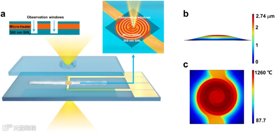
▲ 图1
Simulation of the gas heating chip. (a) Enlarged top view of the nanolab. (b) Thermal expansion at the z axis of microheaters by COMSOL simulation at 1260 °C. (c) Temperature distribution of microheaters by COMSOL simulation at 1260 °C.
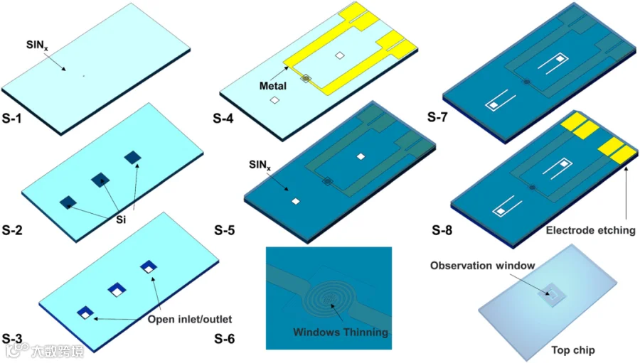
▲ 图2
Nanofabrication processes of the nanolab (S-1 to S-8). The bottom chip is composed of the heating layer, channel inlet/outlet and observation windows made of extremely thin SiNx. The production process of the upper chip is the same as that of the bottom chip but does not include the metal heating layer and the channel opening.
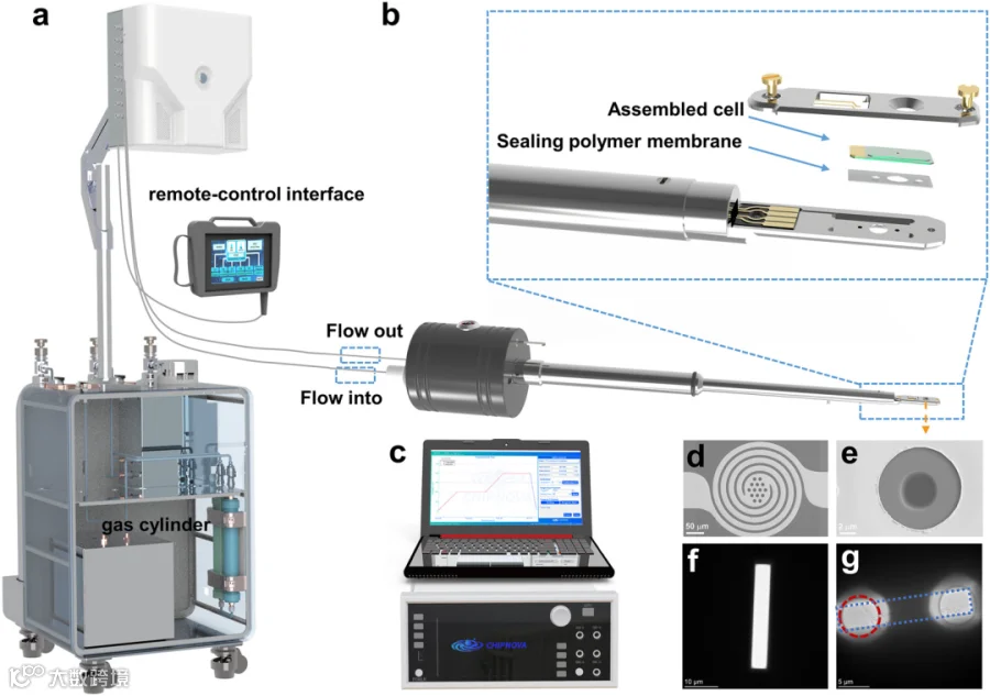
▲ 图3
Illustration of instruments. (a) Schematic illustration of the in situ gas nanofluidic control system. (b) Schematic illustration of the gas flow holder with chips. (c) Temperature control equipment and software. (d) SEM image of the heating wire. (e) SEM image of the observation window.(f) Observation window of the top chip. (g) TEM image of the nanolab window.
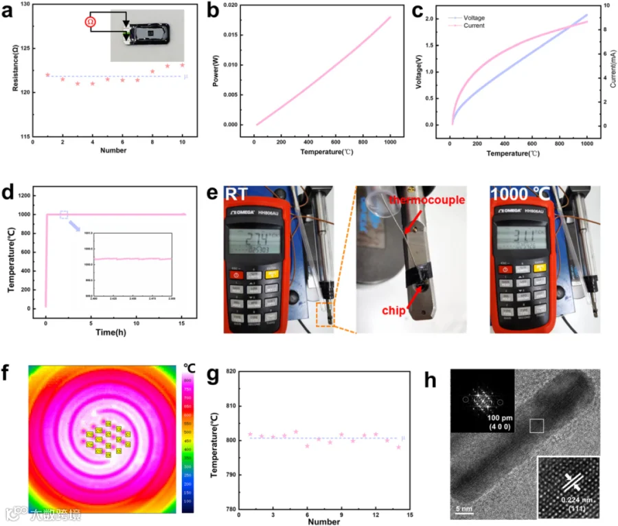
▲ 图4
Heating performance and resolution test. (a) Mean value of the resistance scatter distribution of ten randomly selected chips. (b) Power at different temperatures during heating. (c) Voltage and current at different temperatures during heating. (d) Heating curve at 1000 °C in the TEM and enlargement of the curve. (e) Temperature measurement and the chip thermal insulation performance during heating. (f) Fourteen spots located in the observation windows. (g) Temperature of selected fourteen points. (h) High-resolution image and FFT pattern of Pd nanoparticle at 1 bar of air in the nanolab.
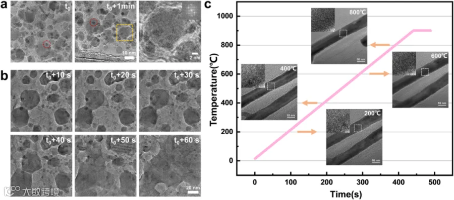
▲ 图5
Drift rate test. (a) High-resolution imaging of alumina nanoparticles during heating and the drift rate within 1 min. (b) The melting and creeping of alumina nanoparticles when the temperature is maintained at 1300 °C. (c) In situ heating of Pd nanowires in the nanolab and highresolution image at different temperatures.
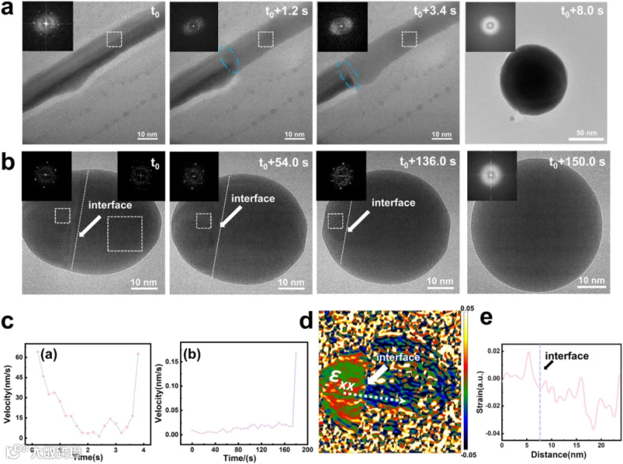
▲ 图6
Pd nanowire reshaping in the nanolab. (a) Image sequences of Pd nanowire reshaping in the nanolab during heating. (b) Image sequences of Pd nanoparticle reshaping in the nanolab during heating. (c)Interface moving velocity in (a) and (b). (d) GPA image of εxx obtained from the TEM image at t0 + 54.0 s in (b). (e). Line profiles of εxx along the direction marked by an arrow in (d).
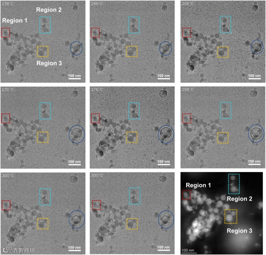
▲ 图7
Reduction of ferric oxide in the on-chip reaction nanolab. Image sequences of ferric oxide at different temperatures in hydrogen and STEM image after reaction.
相关论文信息
原文链接:
https://pubs.rsc.org/en/content/articlelanding/2023/LC/D3LC00184A
(点击文末阅读原文直达链接)