搜索
首页
大数快讯
大数活动
服务超市
文章专题
出海平台
流量密码
出海蓝图
产业赛道
物流仓储
跨境支付
选品策略
实操手册
报告
跨企查
百科
导航
知识体系
工具箱
产业园
更多
找货源
跨境招聘
DeepSeek
首页
>
首揭FD-SOI(全耗尽型绝缘层上硅)技术
>
首揭FD-SOI(全耗尽型绝缘层上硅)技术
芯华舍
2017-06-23
0
导读:近日,虚拟现实产业又正式迎来了一个重磅级新玩家。在WWDC2017全球开发者大会上,苹果正式宣布其Mac和i
来自格罗方德的首席技术官GaryPatton,为我们揭开了FD-SOI技术,与finFETs工艺对比,谁是最适合下一代缩放的技术。与行业半导体工程师主要讨论了FD-SOI技术、集成电路缩放、工艺技术以等话题,以下是此次谈话的内容:
SE:Inlogic,GlobalFoundriesisshipping14nmfinFETswith7nmintheworks.Thecompanyisalsoreadying22nmFD-SOItechnologywith12nmFD-SOIinR&D.WhydevelopbothfinFETsandFD-SOI?
Patton:Wear
epr
ovidingourcustomerswithtechnologythat’sreallyoptimizedfortheirapplications.Wearenottryingtofiteverybodyfromhigh-endserverstobattery-powereddevicesintoonetechnologyflavor.
SE:ThereissomeconfusionwhereFD-SOIandfinFETscompeteinthemarket.Canyouelaborate?
Patton:IamabigfanoffinFETs.Ispendalotofmytimeon7nm.Wearetryingtogetthatreadyforcustomertape-outsearlynextyear.It’sagreattechnologyifyouarefocusedonperformance.Ifyouaremakinglargechipsandyouhavealotofwirecapacitance,youlovethedrivecurrentofafinFETdevice.Butifyouaremakingsmallerchips,wherethegatecapacitanceisabiggerissue,thenthefinFEThasalittlebitofadisadvantage.Also,it’samuchmorecomplexprocess.Noteverybodyismakingamillionwafersfortheirproducts.It’samoreexpensiveprocess.Andithasmorecomplexitywithdouble-,triple-andquadruple-pattering,aswellasthecomplexitieswithRFandanalogdesigninafinFETdevice.
SE:WhataboutFD-SOI?
Patton:FD-SOIisreallyatechnologyoptimizedforthelow-costIoT,battery-powered,low-endmobileandautomotiveapplications.
SE:Doyoupushonetechnologyoveranother?Patton:We’reagnostic.We’renottellingcustomersthatyouhavetodofinFETsorFD-SOI.Wewantcustomerstousethetechnologythatfitstheirapplication.SE:Whoaretheearlyadoptersfor22nmFD-SOI?Patton:Automotiveisdefinitelyoneofthestrong
ones
.T
heca
meraspaceisanother,andsomeofthebattery-poweredIoT.SE:What’shappeninginautomotive?Patton:CertainapplicationsinautomotivearebetteroptimizedforFD-SOIlikeradar.OtherapplicationsmayusefinFETs.SoweareactuallygoingthroughautomotivequalificationinourMaltafabfor14nm.Again,theautomakerscanchoose.SE:GlobalFoundrieshasannounced22nmFD-SOIwithplanstoaddmorecapabilitiestothetechnology,right?Patton:Thebasetechnologyisdone.ThebaseIPdevelopmentisdone.Andnow,weareworkingontheextensions.Webelieveoneofthekillerapplicationsforthisistobeabletodoasingle-chipsolutionfortheIoTspace.That’sRFandeverything.SE:WhatelseareyoudoingwithFD-SOI?Patton:There’sembeddedmemory.WehaveMRAM,whichwewillbringin.And,ofcourse,wehave12nmworkgoingon.
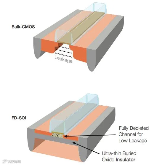
Fig.1:BulkCMOSvsFD-SOI.Source:GlobalFoundries
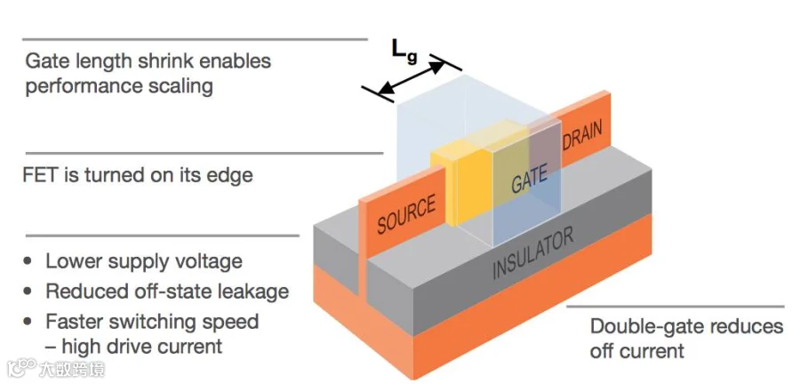
Fig.2:7nmfinFET.Source:GlobalFoundries
SE:ThereisaperceptionthatonlyafewcustomershaveadoptedFD-SOI.WhatarethechallengesofgettingmoreadoptionforFD-SOI?Patton:We’veworkedwithleadcustomersonFD-SOIandtheynowunderstandtheissues.First,therewasthehistoryorconcernsaboutexecution.Wearewellpastthat.Peopleunderstand22nm.It’ssolidtechnologyandit’syieldingverywell.We’veexecutedwhatwe’veplanned.WeknewIPwasgoingtobecritical,becauseFD-SOIisnewanddifferentforpeople.Sowe’vebeeninvestingfromthebeginningontheIPecosystem.OurinitialpartnerwasInvecastohelpbuildupthefoundationalIP.Sincethen,we’vemadeabigincreaseandinvestmentinalloftheIParoundthetechnology.SE:Whatelse?Patton:Bytheway,there’smulti-sourcing.WehaveafabcomingupinChengdu,China.Also,weknowChinawillbeabi
gmarket
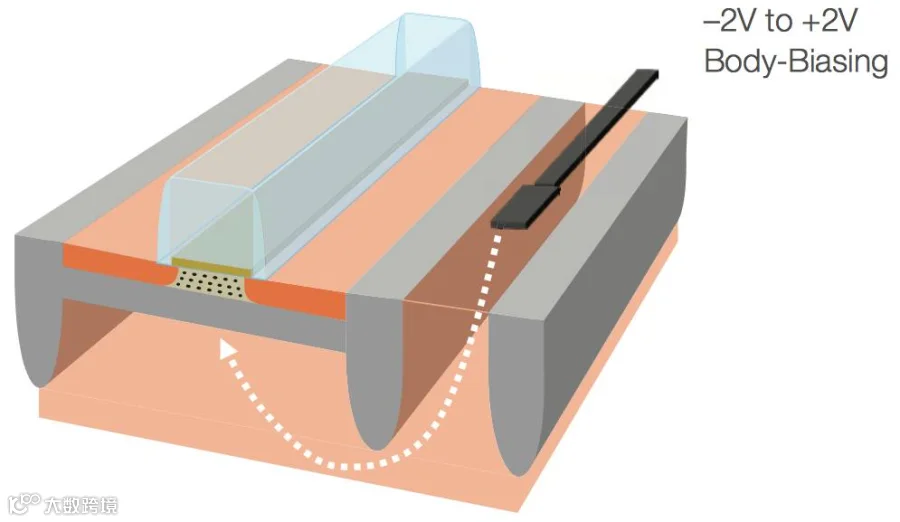
forFD-SOI.That’sbeenprettyclearfromtheconversionswe’vehadwithcustomersinChina.So,wewillhavetwobigfactoriesforFD-SOI—DresdenandChengdu.SE:SomeanalystssayyouneedmoreICdesignresourcestomakechipsaroundFD-SOI,ascomparedtobulkCMOS.Isthatthecase?Patton:That’ssomeoftheFUD(fear,uncertaintyanddoubt)spreadbyourcompetitors.Wehaveprogramstohelpteachourcustomershowtouseback-bias.Anumberofthemarestartingoutwithoutback-bias.Theygetthatundertheirbelt,andthentheycantaketheproducttothenextlevelbyusingback-bias.Someofourecosystempartnersareputtingthetoolsinplace,sothatit’sfairlyeasytodesignwithback-bias.Youdohavetothinkabouthowyouwanttoarchitectthesystem.That’swheretheyprovidetheirvalueintermsofdifferentiationandfiguringouthowtheywanttoleveragethisthingcalledbody-biasatacircuit,blockorchiplevel.
Fig.3:Whatisbody-bias?
SE:Whatabout12nmFD-SOI?Whynotofferthatat10nm?Patton:It’sstillplanarandwehavetogotodoublepatterning.10nmisarepeatofhistoryon20nm.10nmtakesthingsjusttothepointwhereyouneedtriplepatterning.Andsowebackedoffalittleinscalingwithabigmaskcostreduction.Wedon’tinvokeasmanydouble-ortriple-patterninglevels.Soifyoucompareitto10nm,12nmFD-SOIis40%lessmasks.Andour22nmisabout40%lessmasksthan14nm/16nm.SE:ThereisalsoaperceptionthatFD-SOIsuffersfromhighersubstratecosts.Anythoughts?Patton:That’sonlypartoftheequation.Whenyougetabigmaskcostsavings,youaresavingetchsteps,depositionstepsandothers.Itcompensatesforit.
SE:Let’smovetochipscaling.IstheindustrykeepingupwithscalingorMoore’sLaw?
Patton:Itusedtobesimple.Theindustrywasscaling50%andwouldadd10%or15%complexityfora30%to35%diecostimprovement.Butnowyouareadding25%complexity.Let’sjustpickthatasanumber.Now,youareonlygettinga20%diecostimprovement.That’snotquiteasexcitingforsomebodydoingdesign,especiallyifyoulookatthecurvesondesigncosts.Designcostshavebeengoingupatanexponentialrate,sopeoplehavetospendmoretodesigninthisnewtechnology.SE:WhataboutGlobalFoundries’7nmtechnology?Patton:Our7nmisscaled,versus14nm,about0.37x.Wealsoknowtherearemoremasksthan14nm.Attheendoftheday,whenyoutaketheshrinkageandthecomplexityincrease,wearegivingcustomersagooddiecostimprovementfortheinvestmenttheyaregoingtomakeinthedesign.
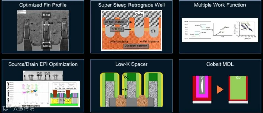
Fig.4:Keyinno
vat
ionsfor7nm.Source:GlobalFoundries
SE:GlobalFoundriesdecidedtoskip10nmandmoveto7nm.Why?Patton:Thescalingfactorfor10nmisprettymodest.It’smoreofahalfnode.Allthethingswe’veheardfromcustomersistheperformanceimprovementfor10nmisprettymarginaloverthepreviousnodein16nm/14nm.Sofor7nm,ifyoulookatscalingandcost,it’shittingthatcosttargetof30%to35%diecostimprovement.SE:Whatarethebigchallengesfor7nm?Patton:Clearly,thecomplexityisrightupthere.Youaretalkingaboutsomethinginthemid-80sformaskcount,whichisprettyamazing.Themiddle-of-
line
isalsoakeychallengingarea.Gettingtotheperformancetargetisthethirdkeychallenge.SE:For7nm,GlobalFoundriessaiditwouldinitiallyuse193nmimmersionandmultiplepatterning,andnotEUV.Isthatstillthecase?Patton:Yes,definitely.Wehaveanumberofproductstapingoutnextyear,includingthefirstoneintheearlypartofnextyear.AndEUVisnotreadyonthattimeframe.WedohaveEUVtoolscomingintoMalta.Wewanttobepreparedforthetransitionbecauseitclearlyoffersadvantages.WehavetwoEUVtoolscominginnextyear,andthenwewillhaveanothertwotoolscomingintheyearafter.SowewillbewelloutfittedwithEUVtooling.WehaveourEUVtool,ofcourse,inAlbany,whichweareusingwithIBMfordevelopment.FormanufacturingwewillhaveEUVcapabilityinplace.Andthenwewilltransitioncustomersandproductsovertothatwhenit’sready.Itwillgiveusacycletimeandadefectdensityimprovement.Andwe’lluseitforashrinkon7nm.SE:SoyouplantoinsertEUVat7nmatsomepoint?Patton:Wewilllaunch7nmwithimmersion.WewillmakesureourgroundrulesarecompatibleinordertomigratelevelstoEUV.Andthen,we’lllookatashrinkonthatattherighttime.SE:Whataboutthefinsat7nm?Doyouneedtomakethemtallertoboostthedrivecurrents?Patton:We’vegoneabittallerwiththefins.Therearesomedisadvantagesofgoingtotallerfins,aswell.Thefinshapeisprobablythemostcriticalone.Gettingthefinprofileshapeiscritical.Also,gettingthatjunctionisolationiskey.Yourfinisisolated,butifyougettoomuchoverlaptothesource-drain,itaddsalotofcapacitance.Thisslowsdownthetransistor.SE:IsGlobalFoundriesco-developing7nmtechnologywithSamsung?Patton:Wearedoingitcompletelyonourown.Wehadthecollaborationon14nm.WestillpartnerwiththemonwhatI’dcallpathfindinginAlbany.AspartofthedealwithIBM,Albanyusedtobeanall-joint-developmentalliance.Thenitwasspiltintotwoparts.Halfofthefacilitycontinuestodothejointdevelopmentwork,whichIBMleads.Thinkofthataspathfindingfor5nmandbeyond.AndtheotherhalfisaproprietaryIBM-GlobalFoundriescorridor,whichisspe
cif
icallyfocusedonacceleratingthingsintoMalta.Thosecouldbeperformanceelementsfor7nmand7nmplus.Infact,Iwouldenvisionwe’llhaveabunchofperformancekickersat7nm.Thiswillbealongnode.
SE:SothefinFETwilllastatleastuntil7nm.Whatabout5nm?Patton:Wehaveworkgoingonthat.Wehaveworkinnewdevicestructureslikegate-all-aroundinAlbany.Somethinkthatyoucangoto3nmwithfinFETs.Iamabitskepticalonthattopic.Wewillneedsomenewdevicestructuresbeforethen.
戳下面的
原文阅读,更有料
!
【声明】内容源于网络
0
0
芯华舍
内容
397
粉丝
0
关注
在线咨询
芯华舍
总阅读
60
粉丝
0
内容
397

 芯华舍
芯华舍