


Figure 1: Interfacing three α-MoO3 slabs with crystal orientations θ1, θ2, and θ3, isofrequency contours, and the Re(Ez) field distribution.
1. Pre-reading
Negative refraction (NR) has a wide range of applications in diverse fields such as imaging, sensing, and waveguides and typically entails the fabrication of intricate metamaterials endowed with hyperbolic features. In contrast to artificially engineered hyperbolic materials, natural van der Waals (vdW) materials are more accessible owing to their inherent strong in-plane covalent bonding and weak interlayer interactions. However, most vdW materials manifest uniaxial crystal properties, which restrict their behavior solely to out-of-plane hyperbolicity. This characteristic poses a considerable challenge to their seamless integration via planar fabrication techniques, unless a suitable pattern is employed. Recent advances have identified natural biaxial α-phase molybdenum trioxide (α-MoO3) as a promising vdW material capable of exhibiting in-plane hyperbolicity.
In this study, the research team led by Prof. Chia-Chien Huang suggested a unique technique in this study for integrating differentially oriented 𝛼-MoO3 slabs covered with a tunable graphene layer on an Au substrate. By tailoring the orientations of the 𝛼-MoO3 slabs and modulating the Fermi energy of the graphene layer, three remarkable outcomes were achieved: broadband and all-angle NR, simultaneous positive refraction and NR, and diffractionless propagation for flexible manipulation of mid-infrared polaritons. The significance of these findings extends beyond the materials and structures considered in this study, as they are potentially applicable to other types of vdW materials.
The proposed mechanism presents an innovative platform for effectively manipulating mid-IR polaritons for further advances in the development of polaritonic devices.
2. Background
NR is a counterintuitive physical phenomenon where the refracted ray of light is deflected to the same side of the interface normal as the incident ray. Subwavelength dielectrics and metallic elements are used to artificially construct hyperbolic media, which are characterized by permittivity tensors with one component along a principal axis having an opposite sign compared to the other two components. However, fabricating hyperbolic media using bulk materials is a major challenge. Therefore, researchers have turned to natural 2D vdW materials, which offer numerous advantages including low-loss characteristics, giant optical anisotropy, and ultrahigh mode confinement for enhanced light–matter interactions. These vdW heterostructures exhibit hybrid properties derived from the unique advantages of their constituent elements, which provide an additional degree of freedom for manipulating optical properties and designing novel photonic devices.
However, uniaxial hexagonal boron nitride (hBN) and certain transition metal dichalcogenides (TMDs) exhibit out-of-plane hyperbolic and in-plane isotropic dispersions. This behavior arises from the permittivity tensors, which possess two negative components in the in-plane direction and a positive component in the out-of-plane direction. The out-of-plane hyperbolicity poses a major challenge for the design of planar photonic circuits. hBN and TMDs require nanostructured patterning to achieve in-plane hyperbolicity, but this introduces surface roughness and defects that increase optical losses. Recently, a natural biaxial vdW semiconductor, α-MoO3, has been discovered that exhibits in-plane hyperbolic dispersion. A twisted bilayer and interface engineering of the structure have been proposed to further manipulate the properties of α-MoO3 and realize exotic phenomena such as topological transitions, wavefront control, directional canalization, and diffractionless propagation. By covering the α-MoO3 slabs with monolayer graphene, their optical properties can be tuned by varying the charge carrier density of the graphene.
3. Innovative research
We investigated NR when two α-MoO3 slabs, both covered by monolayer graphene, were interfaced with different orientations. Figure 2A depicts the left and right slabs in light green and light red, respectively. Under the conditions of ω = 910 cm−1, t= 150 nm, Ef = 0.15 eV, and θ1 = 20°, we investigated the Re(Ez) field distributions and corresponding IFCs for θ2 of −10° to −90°. Figures 3B, 3C, 3F, 3G, and 3H depict the field distributions of Re(Ez) with Pi and Pnt. The black dashed line indicates the interface between the two slabs. Figures 3D, 3E, and 3I–3K depict the corresponding IFCs where they overlapped. Here, we have superimposed the analytically calculated IFCs onto the numerical results, as illustrated in Figures 3D, 3E, and 3I–3K. In the case of the left α-MoO3 slab with a fixed orientation angle of θ1= 20°, we have indicated the inner elliptical and outer hyperbolic IFCs using green dashed lines. For the right α-MoO3 slab, we have indicated the elliptical IFCs with different angles of θ2 using cyan dashed lines. The trajectories of the incident (ki) and refracted (knt) wavevectors are depicted with dashed green and red lines, respectively, while the incident (Pi) and refracted (Pnt) Poynting vectors are represented by solid green and red lines, respectively. The dashed white line represents the fixed y-component (ky) of the incident wavevector, which was preserved as light passed through the interface. Notably, Pnt was refracted toward the opposite side of the interface normal to Pi. Consequently, NR was achieved by manipulating the crystal orientations of the α-MoO3 slab, and the NR angle can be arbitrarily determined by θ2. These results demonstrate the ability of the proposed structure to achieve all-angle NR in the mid-IR regime.
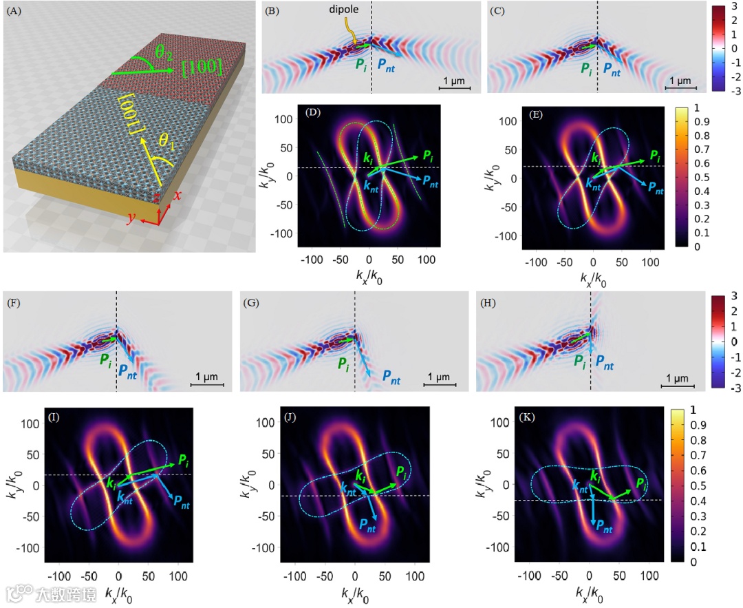
Figure 2: (A) Graphene-covered α-MoO3 slabs with different crystal orientations on an Au substrate, where θ1 and θ2 are the angles between the x-axis and directions of the individual slabs. The left and right α-MoO3 slabs are indicated by light green and light red colors, respectively. Re(Ez) field distributions under the conditions of ω = 910 cm−1, t= 150 nm, Ef = 0.15 eV, and θ1 = 20° at θ2of (B) −10°, (C) −30°, (F) −50°, (G) −70°, and (H) −90° and (D), (E), (I)–(k) the corresponding IFCs, where the green and cyan dashed lines indicate the analytical calculated IFCs of the left and right α-MoO3 slabs, respectively.
Figure 1A shows the extension of the proposed structure to multiple interfaces comprising three α-MoO3 slabs. This configuration allowed the crystal orientations of each α-MoO3 slab to be manipulated and introduced additional degrees of freedom for controlling the optical properties of the system. Figure 1B shows a three-dimensional view of the Re(Ez) field distribution under the conditions ω = 910 cm−1, t = 150 nm, Ef = 0.15 eV, θ1 = 0°, θ2 = −30°, and θ3= 30°. The polariton was split and refracted into two preset transmission directions corresponding to θ2= −30° and θ3 = 30°. Figure 1C visualizes ki and the two transmitted wavevectors kpt and knt, where kpt is the positive refraction in the IFCs derived from the three differently oriented α-MoO3 slabs. The corresponding Pi, Ppt, and Pnt are also indicated, where Ppt is the positive refractive Poynting vector. Figure 1D shows a top view of the Re(Ez) field distribution and highlights the power flows represented by the Poynting vectors Pi, Ppt, and Pnt.
To further control the polaritons, we interfaced two α-MoO3 slabs partially covered with graphene, as shown in Figure 3A. The left α-MoO3 slab had a crystal orientation of θ1 = 0°, as shown in Figure 3B, and was completely covered with monolayer graphene, which was electrically gated with Ef1. The right slab had the crystal orientation θ2, and it was partially covered with graphene, which was electrically gated with Ef2. The separation between the graphene layers was denoted as S. A z-polarized electric dipole was positioned at a distance of d= 1 µm from the left interface on the x-y plane. The other conditions were set to ω = 910 cm−1, t = 150 nm, S = 1 µm, Ef1= 0.3 eV, θ1 = 0°, and Ef2 = 0.25 eV. Figure 3C to 3E display the Re(Ez) field distributions for θ2= 0°, 20°, and −20°, respectively. The partially covering graphene on the right α-MoO3 slab with a suitable Ef2 = 0.25 eV overcame the diffraction of the light beam, and diffractionless propagation was achieved.

Figure 3: (A) Interfacing two α-MoO3 slabs, in which the left slab is entirely covered with graphene (Ef1) but the right slab is partially covered with graphene (Ef2). (B) The same as (A), except peeling off the graphene layer to clearly show the orientations of α-MoO3 slabs. The two graphene layers have a separation distance of S = 1 µm, where θ1 = 0° (left slab) and θ2 = 0° or −20° (right slab). Re(Ez) field distributions for various cases: (C) θ1 = 0° and θ2= 0°, (D) θ1 = 0° and θ2 = 20°, and (E) θ1= 0° and θ2 = −20°. (F)–(H) Corresponding |E| fields.
4. Applications and perspectives
We demonstrated the feasibility of interfacing differently oriented α-MoO3 slabs covered with tunable graphene on an Au substrate to realize NR. Three remarkable outcomes were achieved: broadband and all-angle NR, simultaneous positive refraction and NR, and diffractionless propagation for flexible manipulation of mid-infrared polaritons. The integration of multiple α-MoO3 slabs opens up exciting approaches for designing and implementing photonic devices such as beam splitters and Mach–Zehnder modulators. Therefore, the proposed approach also opens up the possibility for diffractionless propagation in imaging systems and steering the diffractionless beam in wide angles to any desired direction by presetting the crystal orientation by controlling the geometry and material parameters. Our proposed mechanism presents an innovative platform for effectively manipulating mid-IR polaritons for further advances in the development of polaritonic devices.
These research results are published online with the title "Interfacing differently oriented biaxial van der Waals crystals for negative refraction" on Nanophotonics.
The authors of this article are Ruey-Tarng Liu and Chia-Chien Huang. Chia-Chien Huang is the corresponding authors of this work. Prof. Chia-Chien Huang's research group is affiliated to the Department of Physics and Graduate Institute of Nanoscience, National Chung Hsing University, Taiwan.
